Chip War Heats Up: AMD's RDNA4 Navi 48 Packs Punch with Unprecedented Transistor Density

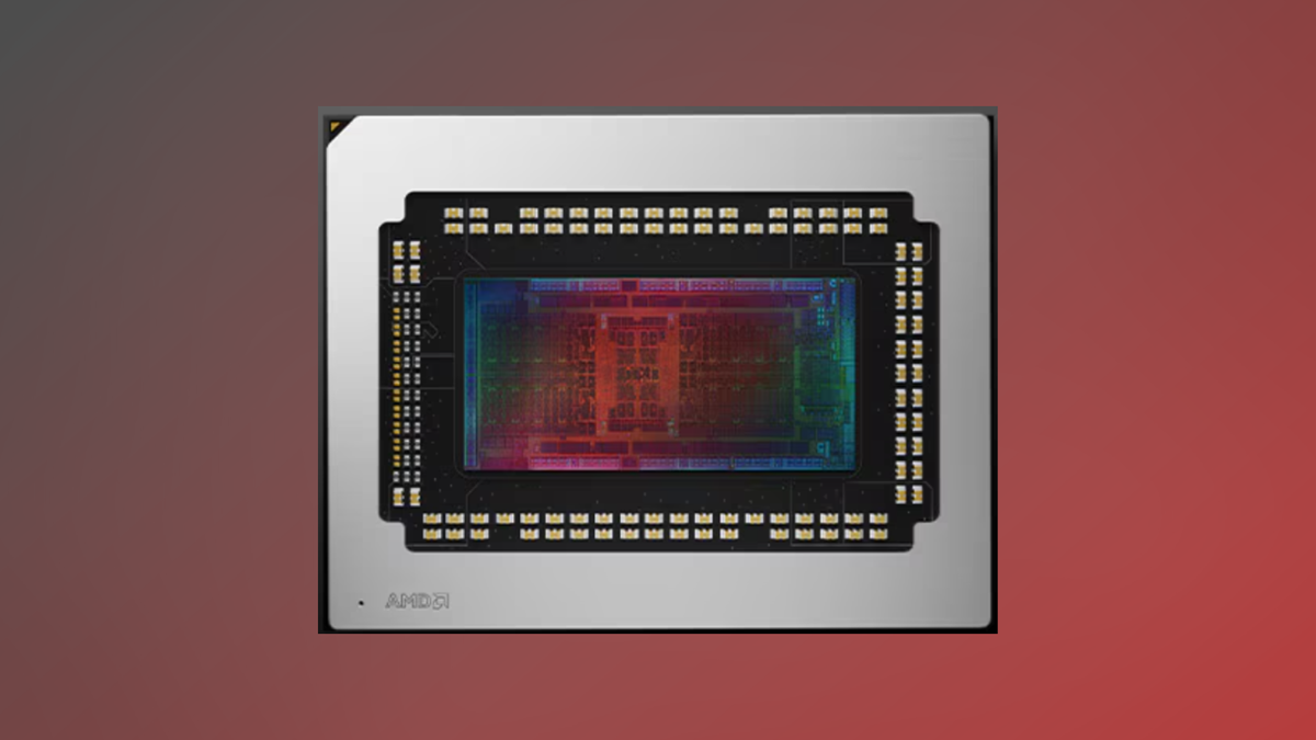
Breaking new ground in semiconductor technology, engineers have achieved a remarkable milestone: cramming an astounding 150 million transistors into every square millimeter of silicon. This groundbreaking advancement not only pushes the boundaries of miniaturization but also creates exciting possibilities for integrating advanced features like L3 cache directly on the processor die. By packing transistors with such unprecedented density, chip designers are unlocking new potential for faster, more efficient computing architectures. The ability to incorporate L3 cache within the same silicon real estate means dramatically reduced data transfer latencies and improved overall processor performance. This technological leap represents a significant step forward in the ongoing quest to make computing components smaller, more powerful, and increasingly sophisticated. As transistor density continues to increase, we can expect even more impressive computational capabilities in future generations of processors and electronic devices.

Revolutionizing Microchip Technology: The Breakthrough of Nanoscale Transistor Density

In the rapidly evolving landscape of semiconductor technology, a groundbreaking advancement promises to redefine the boundaries of computational power and miniaturization. Engineers and researchers are pushing the limits of what was once considered impossible, creating a new paradigm in integrated circuit design that could transform multiple industries.

Pushing the Boundaries of Technological Innovation: Where Microscopic Meets Miraculous

The Quantum Leap in Transistor Miniaturization

The world of semiconductor engineering stands on the precipice of a transformative breakthrough that challenges our fundamental understanding of computational architecture. Traditional limitations of chip design are being systematically dismantled through unprecedented engineering precision. Researchers have developed a revolutionary approach to integrating an astounding 150 million transistors within a single square millimeter of silicon, a feat that seemed inconceivable just a few years ago. This extraordinary density represents more than a mere numerical achievement. It symbolizes a quantum leap in our ability to compress computational power into increasingly smaller physical spaces. By strategically embedding Level 3 cache directly onto the die, engineers have created a more efficient, streamlined architecture that dramatically reduces signal transmission distances and enhances overall processing capabilities.

Architectural Implications of Nanoscale Engineering

The implications of such dense transistor integration extend far beyond simple numerical improvements. By radically reducing physical dimensions, semiconductor designers unlock potential for exponentially more powerful computing systems. Each nanometer of reduction represents a potential geometric increase in computational capacity, opening doors to unprecedented technological applications. Thermal management becomes a critical consideration in these ultra-dense chip designs. Traditional cooling mechanisms become increasingly challenging as transistor density increases, requiring innovative solutions that can dissipate heat efficiently without compromising performance. Advanced materials science plays a crucial role in developing substrates and thermal interfaces that can handle these extreme computational environments.

Future Technological Ecosystems

The ramifications of this technological breakthrough ripple across multiple domains. From artificial intelligence and machine learning to quantum computing and advanced scientific simulations, ultra-dense transistor configurations promise to accelerate computational capabilities in ways previously unimaginable. Emerging fields like neuromorphic computing and edge artificial intelligence stand to benefit immensely from these advancements. By creating more compact, energy-efficient computational units, researchers are laying the groundwork for next-generation smart devices that can process complex algorithms with unprecedented speed and efficiency.

Global Competitive Landscape

This technological milestone represents more than a scientific achievement—it's a strategic imperative in the global technological arms race. Nations and corporations investing in advanced semiconductor research are positioning themselves at the forefront of future technological innovation, recognizing that computational density is a critical metric of technological leadership. The economic implications are profound. Companies that can successfully implement these ultra-dense transistor configurations will gain significant competitive advantages, potentially reshaping entire industrial ecosystems and creating new paradigms of technological capability.